Casting Wolf3D-style Rays with an FPGA and Arduino
By dormando
Classical raycasting engine using embedded microcontrollers and FPGAs.
This project pairs a standard arduino (ATmega328) with a small Field Programmable Gate Array (ICE40LP8K) on two small boards, outputting to a 320x240x16bit SPI LCD. Using a mix of C and Verilog for implementation.
This post walks through the separation of duties between the Arduino and FPGA, optimizations to the raycasting algorithm, and other details. It doesn’t assume prior knowledge of FPGA’s or Verilog, but reading some links along the way will make it easier to understand.
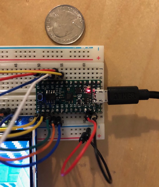
The full setup. Pen for scale.
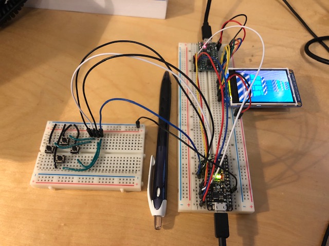
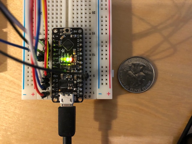
The brains/MCU are an adafruit metro mini:
The “GPU” is a TinyFPGA BX. A programmable microchip - the actual chip is that tiny square in the very center of the board.
Code Repository: https://github.com/dormando/tinyfpga-raycaster
Parts list:
- breadboard(s)
- jumper wires
- 22 gauge solid core wire
- standard push-buttons
- adafruit metro mini: https://www.adafruit.com/product/2590 chosen because its voltage can be selected to 3.3v, needed to talk to the FPGA.
- TinyFPGA BX: https://www.crowdsupply.com/tinyfpga/tinyfpga-bx - chosen due to low cost, small size, and Open Source toolchain.
- 2.2” LCD: https://www.adafruit.com/product/1480
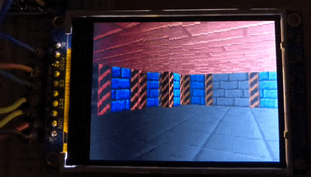
Game textures are public domain, from the game LAB:
 all textures from  my game LAB

 in case you never heard of it it's a little Wolf3D clone made in Flash AS3
 ( and you can play/download it for free: https://mutantleg.itch.io/lab )

 all these gfx is hereby public domain (CC0)
 (credit is not required but much appreciated indeed)

  game and graphics by Mutantleg (me)  (2015)
Background and Motivation
Late last year I picked up an old game programming book from my shelf and gave it a re-read for fun. I’d also read through the (second ed.) of the Wolfenstein 3D Game Engine Black Book. Going back to roots of the 3D game revolution. I recall playing Wolf3D when it was new; definitely amazing for its time.
Earlier last year I’d also picked up a hobbyist FPGA: “mojo v3” sporting a Xilinx spartan-6 clocked at 50mhz. Sadly the toolchain it used was crufty abandonware from Xilinx (a miserable pile of TCL?) but it was fun to play with.
The combination got me thinking: What if someone designed a GPU for a Wolf3D engine? As though they made a game cart with an extra chip like in the 8/16bit console days? Of course you would never do it; if you had custom silicon available you’d just make Star Fox - nevertheless I found the idea fascinating.
Lots of people have implemented raycasters on Arduino’s. Here’s a pretty impressive example of one - It does look good and has a surprising number of features. However the 1 bit graphics and low resolution show the limits of the device.
The first pass at this project was completed a few months ago. The entire stack is implemented on an FPGA: raycaster, line drawing, various drivers. Interacting with it required some programs running on a PC, with bootstrapping involving running several perl scripts in order. It wasn’t quite what I originally envisioned, but I got much farther than I expected. It worked! It also took a long time. Diving into raycasting immediately after making a light blink may not have been the best idea. Verilog is slow to write and the tooling is odd, but I got a very thorough refresher on some CS fundamentals.
Recently I acquired the TinyFPGA BX; a weaker FPGA compared to the original Xilinx Spartan-6. Clocked lower (16mhz vs 50mhz), with less logic and no hardware multiplication (DSP’s). However the chip was newer and its toolchain fully Open Source. I decided to port the project and do it properly this time.
This version runs at the same speed as the original startan-6 build, but moves a lot of the logic onto an Arduino. This is true to my original goal of making an independent game device, and made the project code a lot easier to follow.
The Engine
Writing a ray casting engine is a rite of passage for many people. Despite owning the old books I’d never managed to write one myself. Instead I decided computer networks were “neat”. I’m still trying to figure out if that was a mistake.
There are two typical approaches to raycasting engines. One, based off the original Tricks of The Game Programming Guru’s book, as detailed by Permadi in 1996. The other is known as the lodev tutorial. The latter is a more clear approach with straightforward code.
I went with the lodev version of the algorithm for this project. I did later realize one benefit of the original algorithm: while it requires “fisheye lense” correction for the projection, it can also use small lookup tables for most calculations. For the lodev case there were a number of divisions, which are painful for FPGA’s and microcontrollers.
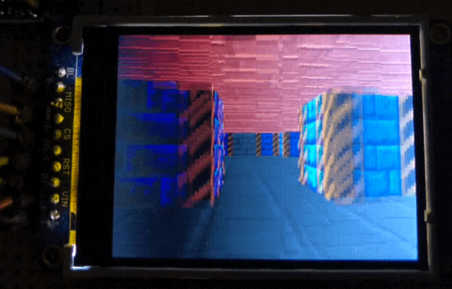
Sprites are not implemented, but texturing for floors, ceilings, and walls are all working.
The Hardware
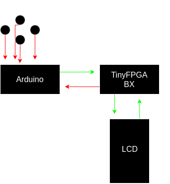
Most of the devices in this stack communicate with each other via SPI protocol. Arduino <-> FPGA and FPGA <-> LCD.
A standard Arduino is an 8-bit microcontroller with low specs, a handful of pins, and big fun. I chose the Metro Mini from Adafruit as a solder bridge could be adjusted to switch the pin voltage to 3.3v, matching the TinyFPGA BX. A normal arduino works too, but you need to wire up a bunch of resistors as voltage dividers to convert the 5v signal.
- 8-bit CPU
- 16mhz clock
- 32K of flash program memory
- 2K of SRAM
- Hardware SPI/serial pins
The FPGA is a TinyFPGA BX, sporting an ICE40LP8K chip.
- 16mhz clock
- 7,680 four-input look-up-tables
- 128 KBit block RAM (16K)
- 41 user IO pins
- 8 MBit of SPI Flash (6 MBit usable by an application)
The 7,680 lookup tables are all the “programming” space available on the FPGA. Every piece of logic (if this, add that, multiply by this) takes up lookup table space. A high speed divider could take up to half of this logic on its own! This project is using about 3,000 LC’s as of this writing. It’s not very well optimized for size yet.
It also has a fair amount of RAM compared to the Arduino (16K vs 2K), but using RAM in an FPGA is a manual process :)
The screen is a 2.2 inch TFT running at 320x240x16bit over an SPI interface.
Astute readers may immediately notice; 320x240x2 bytes is 153,600 bytes. A raycasting engine requires a frame buffer since the lines are drawn vertically. You have 2K and 16K of RAM, so now what?
Normal screen -> 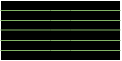
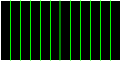 <- This weirdo LCD.
Well, turns out with this LCD you can configure it to render scanlines in any direction you want. Where a VGA monitor has horizontal scanlines, our LCD now has vertical ones! From there, the engine was redesigned to draw one scanline at a time. With this, all of the buffers fit.
The Tooling
I started with the APIO tooling wrapper as described by the TinyFPGA BX guide - this worked well for a while.
Eventually I was having trouble getting APIO to build a working image. I would upload to the FPGA and it would mysteriously fail. Changing random lines in trivial ways would make it work again.
The tooling for an FPGA have a very complicated job: take a mess of descriptive logic, turn it into wires that flip bits around, and lay them out on a chip so everything physcially fits in a magic silicon rectangle. I’ll go into more detail later, but a big deal with this chip layout is the amount of time it takes for a signal to move around the chip electrically. If the tools are creating very long wires or layered logic, the signal may not be stable before the end of the chip’s clock cycle. This leads to failure.
The Arachne-PNR (place & route) tool which came with APIO apparently does not take timing into account when laying out a chip! This was surprising to say the least. Thankfully NextPNR is its rapidly maturing replacement. This new tooling works much better.
In the end I have a simple build.sh file that glues these tools together. I
installed them via the git clone instructions at the project
icestorm homepage
Diagrams
The connections are electrically very simple, with no parts other than wires. The power lines are omitted and not all wires visualized here.
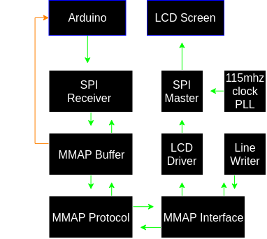
Below is a simplified diagram of the Verilog modules within the FPGA and now they interact with each other and the Arduino/LCD. Some of these modules (MMAP Buffer, Line Writer) contain memory modules or lookup table ROM’s.
The MMAP Buffer module holds bytes while the protocol module waits for the interface module to be unbusy. The buffer module also informs the Arduino when it’s empty, allowing it to wait for the previous frame to flush to LCD before starting a new one. The interface module is the central handler for the FPGA: instructing lines to be drawn or flushed to the LCD.
A Phase Locked Loop within the FPGA creates a secondary 115mhz clock out of its original 16mhz clock. This is used to drive the LCD’s SPI as fast as it’ll go before failing to synchronize.
The Arduino
First lets walk through the responsibilities given to the Arduino, since the FPGA is just doing its bidding. The Arduino takes care of a few things:
Startup:
- Reset the FPGA to a blank state
- Issue initialization commands to the LCD via the FPGA
- Load textures and palettes into the FPGA block memory
Game loop:
- Handle the raycasting calculations
- For each ray cast, ship information to the FPGA to draw and texture a scanline.
- Read button state
- Track player position, translation/rotation of view based on buttons pressed.
If work continues… sprite calculations, game AI, and so on would also be handled by the Arduino.
On a first pass I simply ported the lodev code over with minimal changes. This worked, but was extremely slow: several seconds to render a single frame. First I’ll quickly walk through the startup code, then will go over optimizations and lookup tables for speeding up raycasting on the Arduino.
Initialization
- Reset the FPGA
Resetting is easy enough. When uploading new code or simply turning on the devices, it allows the Arduino to ensure the FPGA is in a consistent state before issuing commands. It does this by holding a special pin high for a few seconds, though a few milliseconds are probably more than enough.
- Issue init commands to the LCD
We’ll talk about the FPGA protocol later, but one feature is the Arduino is able to send commands to the LCD the same as if it were connected directly. This simplifies the FPGA logic a bit, letting the Arduino read the init commands out of its flash memory. It configures the bit depth, gamma levels, screen orientation, and a few other things.
Technically the Arduino can directly issue draw commands as well. This might be a fun way of adding a status bar in the future. The LCD allows you to define a rectangular area to actually draw in. The FPGA would do its big drawing into the main space, and the Arduino would update a few small boxes in the status window perhaps once per second.
- Load textures and palettes
Originally the textures were all 64x64 with their own 256 color palettes. This would only allow 2 or 3 textures to fit in memory on the FPGA, so I decided to cut it down. The textures are scaled down to 32x32 with a 16 color palette, making them 4 bits per pixel. Now each texture only takes 512 bytes for the texture + 32 bytes for the palette. They are also rotated sideways, so a vertical stripe can be read linearly.
The TinyFPGA BX has a relatively large flash chip, with up to 6 megabits available to the user. This would be a much better place to store the textures. Since I haven’t set up a driver for FPGA to do this, it’ll have to wait for another time.
Game Loop
For each frame, the Arduino walks from 0 to 320 (the width of the screen), running the ray calculations. As it finishes each calculation it ships a command to the FPGA to draw a line. It then checks if any buttons are pressed and updates the player position as required.
For a weenie little 8-bit AVR, 32bit floating point math requires some hoops to jump through. Just adding two numbers can take hundreds (or thousands) of cycles. Instead I’ve used an old trick of converting the math to Fixed Point math, in Q8.8 format. Meaning the numbers are now 16bit, with 8 bits representing the whole numbers, and 8 bits the fraction. Q24.8 or Q16.16 would make some things easier, but we would lose some speed again.
Casting a Ray
Compare the code we’re about to walk through with the lodev article (including floors/ceilings). The flow is identical, but the math has changed.
Follow along on github as well - note the code in github may have changed since writing this post.
First we initialize some timers. This is how I profiled which sections to focus on. Then, start a loop; one ray cast for each vertical line.
void castRays(void) {
  unsigned long elapsed = 0;
  unsigned long waited = 0;
  unsigned long DDA = 0;
  unsigned long DDA_start = 0;
  for (int16_t x = 0; x < WIDTH; x++) {
This next bit has a commented function, then the real function is a lookup
table in the Arduino’s flash, which is accessed by byte address. I’ve left the
original function here to show how it would be done without the lookup table.
I added tables in places which have the highest impact. In this case the table
is never going to be more than WIDTH * 16bits in size and it kills a
division.
In the case of our poor 8-bit AVR, dividing 32bit numbers is fairly slow. Doing divisions at all is fairly slow. By comparison it doesn’t seem too bad at multiplication.
    //int16_t cameraX = fixed_div32(((int32_t)(2 * x)) << 8, WIDTH_FIXED) - 0x0100;
    int16_t cameraX = pgm_read_word_near(camerax_data + x);
Next we have some preparation code. The result of our lookup table is multiplied against our current player angle (dirX/Y, planeX/Y), both in Q8.8 fixed point format. Then a few other variables are initialized.
    int16_t rayDirX = dirXF + fixed_mul(planeXF, cameraX);
    int16_t rayDirY = dirYF + fixed_mul(planeYF, cameraX);
    // Avoid some divide by zero's later.
    if (rayDirX == 0) {
      rayDirX = 0x0001;
    }
    if (rayDirY == 0) {
      rayDirY = 0x0001;
    }

    // current map box.
    int16_t mapX = (posXF & 0xFF00);
    int16_t mapY = (posYF & 0xFF00);

    // length of ray to next x/y side.
    int16_t sideDistX;
    int16_t sideDistY;
A quick aside: fixed point multiplication is slightly harder than normal multiplication. To multiply two 16bit numbers without overflow, you must multiply into a 32bit number then shift it back to the right by 8. This is thoroughly explained here for the curious.
int16_t fixed_mul(int16_t a, int16_t b) {
  return (((int32_t)a * (int32_t)b) >> 8);
}
… back to the main code, we take the inverse of the ray direction as the
delta distance between X/Y squares on the map. If you’re following along with
lodev, you’ll notice the original code was simply abs(1 / rayDirX). Later in
the algorithm lodev calls for a division of rayDirX/Y to find the wall
distance. Instead, we hold onto the original inverse along with the absolute
value and turn this into a multiply instead.
Unfortunately I’ve not thought of a way of turning this division into a lookup table. Given how the lodev algorithm works with projecting a plane out from the primary angle, there are many possible angles in a full circle. Perhaps someone with a better understanding of basic math could suggest something. :)
Otherwise, as we’ll see below, these are the only two divisions necessary to cast a ray!
    // use the Norm's as inverses of rayDirXY and avoid a division below.
    int16_t deltaDistXNorm = fixed_div(1 << 8, rayDirX);
    int16_t deltaDistX = abs(deltaDistXNorm);
    int16_t deltaDistYNorm = fixed_div(1 << 8, rayDirY);
    int16_t deltaDistY = abs(deltaDistYNorm);
I’ll skip the next setup bits, as they are identical to lodev aside from being
in fixed point format. The only change of note is addition of sideStepX/Y to
remove another division later on.
Now, the main DDA loop. The amount of time spent in here will vary by the
distance the ray travels to a wall. Overall this takes less than half of the
time of the ray calculation. When this bit was in Verilog for my original
raycaster, I had it optimized to doing an entire DDA check, the whole inner
loop here, in a single cycle! It could finish the entire DDA loop in less time
than it takes the Arduino to multiply some numbers.
If I want to get more framerate out of this design, I will have to move everything from this point below back into the FPGA. The Arduino would calculate the primary rays, do its two divisions, and ship the results off. In the meantime this is clearer.
You can use dividers on FPGAs as well. My original project used a divider “core” generated by the Xilinx tooling and ran the entire ray calcuation on the FPGA along with some lookup tables. It was a sad closed source blob. I can also learn how to create simple dividers on my own, which seem like fun for a future project. Have to keep in mind how limited the logic area is on the ICE40K chip though.
    // DDA loop.
    //DDA_start = micros();
    while (hit == 0) {
      // jump in X or Y direction.
      if (sideDistX < sideDistY) {
        sideDistX += deltaDistX;
        mapX += stepX;
        side = 0;
      } else {
        sideDistY += deltaDistY;
        mapY += stepY;
        side = 1;
      }
      if (worldMap[(mapX >> 8)][(mapY >> 8)] > 0) hit = 1;
    }
    //DDA += micros() - DDA_start;
Original lodev comment; noting the benefit of his algorithm for not having to do a secondary angle correction. I’ve also left the original divider in comments. We now multiply by the inverse.
    // Calculate distance of perpendicular ray (Euclidean distance will give fisheye effect!)
    //if (side == 0) perpWallDist = fixed_div((mapX - posXF + sideStepX), rayDirX);
    //else           perpWallDist = fixed_div((mapY - posYF + sideStepY), rayDirY);
    if (side == 0) perpWallDist = fixed_mul((mapX - posXF + sideStepX), deltaDistXNorm);
    else           perpWallDist = fixed_mul((mapY - posYF + sideStepY), deltaDistYNorm);
We have one other big lookup table; converting the wall distance to a line height, a texture scaler, and an inverse wall distance. The texture scaler is used by the line drawer to grow or shrink the wall texture onto the line. The inverse distance is used by the floor and ceiling calculations.
    // grab a few divisions out of a lookup table.
    // index via 10 bits of perpWallDist.
    uint32_t inverseIdx = ((perpWallDist & 0b0001111111111000) >> 3) * 3;
    int16_t lineHeight = pgm_read_word_near(pdist_to_height_data + inverseIdx++);
    int16_t texScaler  = pgm_read_word_near(pdist_to_height_data + inverseIdx++);
    int16_t invWallDist= pgm_read_word_near(pdist_to_height_data + inverseIdx);
The rest of the code isn’t much different, so I’ll omit it. We’re done raycasting with fixed point math! Wohoo! The Arduino can do this 320 times in roughly 60 milliseconds. The other 30 milliseconds are unfortunately tied up in SPI. As shown below, a lot of the results now need to be shipped to the GPU so it can draw a line.
Originally the primary positions were also shipped for every ray, but that only needs to be sent once per frame. There are some notes for how to reduce it further. If I move the entire DDA calculation back into the FPGA, all we would need to ship are the inverse of the rays and the map position once per frame. The FPGA can calculate the absolute values and any other information by moving the big lookup table over there.
For 320 lines, shipping this data via SPI is roughly 30 milliseconds. Giving us about 90 total milliseconds per frame on average. The SPI bus is also running at 4mhz, since the SPI driver on the FPGA side requires cutting the clock cycles to 1/4th. Speeding this up to the Arduino’s max possible 16mhz may also cut the time here down.
    BXRegister(0b11000100, 4, 0);
    // TODO: just ship lineHeight
    // do draw start / end calc (with div 2)
    // + internal lookup table for inverse dist
    BXData(((uint32_t) drawStart << 16) | (uint32_t)drawEnd);
    BXData(((int32_t) texScaler << 16) | (int32_t)texInitial);
    // TODO: texX is 5 bit, texNum is 8 bit. combine into same 16bit half.
    // then combine with invWallDist, cut SPI traffic by 4 bytes.
    BXData(((uint32_t) texX << 16) | (uint32_t)texNum);
    // Q8.8 for floorXYWall
    BXData( ((int32_t)(floorXWall) << 16) | ((int32_t)(floorYWall)));
    BXData(invWallDist);
Overall, not bad!
The final major bit is I’ve left the game map in RAM… taking up 1200 bytes of the precious 2,048. This is movable to Arduino’s flash, but I haven’t had the need to fix yet.
The FPGA
I won’t really go into how an FPGA works. I’ll stick to the high level of how the logical modules work and interact with each other. If you’re curious in learning, I liked the Alchitry tutorials which were originally for the Mojo v3. I’ve also purchased their latest FPGA’s, which seem like fun products :)
Most books I could find on FPGA’s are either very basic or are academic textbooks. I did find Verilog By Example to be a slightly too light on details but otherwise excellent explainer into the Verilog language. Nothing really clicked for me until I read this super short book.
fpga4fun is also a good resource for learning the basics.
This design is much simpler than my first attempt. I removed partially working sprite modules, and moved the raycasting to the Arduino, as well as gave it the responsibility for managing frames. All the FPGA does at this point is draw lines to an LCD.
A word of warning! I am a complete beginner at logic design! It’s cool to get ideas but you shouldn’t use my source as a way of learning Verilog. After struggling for months with the original project, I’ve learned that if I were to do it properly it would look completely different than this. The modules are far too large and complicated.
Logical Parallelism
Writing Verilog is a real trip. While it can look like normal code, it’s executed any way but normally. Verilog is organized by electrical signals and clock pulses. Some modules may not need a clock at all, IE: combinatorial logic taking two input signals and AND’ing them onto an output signal. Everything else works by the pulse of a clock.
The fundamental building block is a Flip Flop. The above links will explain it much better than I ever could, but in simplest of terms: A Flip Flop in an FPGA has an input D, that gets copied to output Q when the clock pulses. Without this, the electrical state of the circuit would be immovable! Verilog takes care of autogenerating structures of Flip Flops and circuits to satisfy lines such as “A + B” or “A * C” or “if (foo)” and so on.
Say you write a line: c = a * b; in Verilog. In order to synthesize this
onto the chip the tooling must generate a complicated multiplication circuit.
This takes up a fixed amount of space on the chip.
Why is this a problem? Well if you were doing c = a * b; on every cycle,
it’s perfectly fine. However, if you’re doing c = a * b; and then going into
a loop for 10,000 cycles, it can be a huge waste.
This might make it clear why I opted to move the raycaster logic back to the Arduino. While the DDA loop makes sense, there’s a lot of setup and teardown logic which would barely ever get activated.
Further, since the only logic you can typically use is what the chip can electrically “execute” within a single clock cycle, doing more complex work requires state machines. Anyone who’s written asynchronous event based code will know how this ends.
This seeming drawback gives the FPGA its extreme power. So if c = a * b; can
be executed on every cycle, can I do 10 of these multiplications on every
cycle by putting down even more logic? The answer is yes! Now you’re cheating
with logic!
Module Level Parallelism
Since I’m not very good at this, the level of parallelism in this design tends to be at the module level.
If we look at this diagram again:
- The input SPI module can activate at any time; reading bits from the Arduino as it sends them.
- The buffer module can queue bytes from SPI or ship bytes to the protocol module at any time.
- The protocol handler can gather bytes into coherent packets any time the mmap interface allows it to.
- The mmap interface kicks off other modules to run in parallel, sometimes blocking on them to finish work. It also internally handles flushing lines to the LCD.
The line writer module is a little special. A line is 240 pixels high (480 bytes due to 16bit pixels). The line writer actually has a 960 byte circular write buffer. The block RAM in the FPGA can be written to and read from at the same time (within some level of sanity). This allows the line writer to “draw” into half of its buffer while the interface module “flushes” the other half to the LCD.
In other words: The Arduino can write commands while the line writer plots a line while the LCD driver flushes the previous line to the screen, all at the same time on every clock cycle.
Ultimately in this setup everything bottlenecks on the LCD driver. While I’ve clocked the SPI as high as it’ll go, writing bits at a time over a single wire has its limits. There are similar LCD’s available (with the same chip driver, even) which use 8 parallel data pins to communicate instead of the single SPI wire. With one of these the bottleneck would easily move back to the Arduino.
I thought it would be fun to see how far I can push the SPI LCD though. Turns out, pretty far!
Cross Clock Domains
This is a heavy topic that I’ll touch on briefly. With FPGA’s it’s possible to drive multiple clocks internally via Phase Locked Loops (PLL’s). These multiply, divide, and re-synchronize the original clock into a new one. You might recognize these from trying to overclock your poor desktop CPU.
Really beefy FPGA’s can have several PLL’s driving varying clock speeds. There are some limits though:
- The maximum clock rate you can run an FPGA design at is dependent on how deep and complex your logic is.
- EX: If a base clock of 16mhz can multiply two values and add them to a third, there’s no guarantee the chip can accomplish this same level of logic in half the time if you raise the clock to 32mhz.
- Further, modules driven by different clocks won’t be in sync with each other. How can they signal or transfer data?
Which means if you want to really crank up the speed, the logic needs to be as simple as possible.
The signalling and data transfer issues are a large, complex, and deep area of logic design. I’ll just say that I took a simple approach here and isolated the faster clock to the smallest possible area: The SPI module used within the LCD driver module.
In the end, a few clock cycles are lost synchronizing data to the SPI module, but overall everything is lightning fast compared to the default clock rate.
Line Drawing
To round out this explainer I want to go over the line drawing module in detail. The module has a lot of variables but is relatively simple. It takes place of the “okay now for loop a line into the frame buffer” part of the lodev algorithm.
Follow along with the file on github - though again note it may have changed since this writing.
The first 100ish lines of line_writer.v are definitions (localparam is
similarish to #define in C), and Verilog’s version of variable declarations.
Again I’ll butcher the definition, but wire’s tend to connect things
together (modules, pins), while reg’s (registers) are closer to a
traditional variable.
Surprisingly there are a lot of styles for how people write Verilog. Some
styles rely on the tooling inferring FlipFlops, some spell them out more
explicitly. I’ve gone with the latter in this case. Almost all of the
variables are defined twice: once with a _d and once with a _q suffix. The
q registers contain the variable state from the previous clock cycle. The d
registers contain the state for the next clock cycle. d is rarely, if ever,
used within the same cycle.
Meaning if you want to increase a counter a, you do something like: a_d = a_q + 1
I haven’t yet figured out why some people use this style vs others, but it was one I was able to wrap my head around and get to actually work. It does help clarify the logic.
[snip]
localparam FLOOR_OFFSET = 6144;
localparam CEILING_OFFSET = 7168;
localparam FLOOR_PAL = 96;
localparam CEILING_PAL = 112;

reg [3:0] state_d, state_q;
reg [7:0] count_d, count_q; // number of pixels filled
reg [7:0] texid_d, texid_q;
[snip]
Next are a handful of RAM modules. The first is the circular line buffer; holding up to two scanlines worth of data. The line writer draws from the ceiling pixel downward (huh?). It seems like it would make more sense to immediately write the bytes to the LCD as they’re drawn here. Given the way it’s used now that would make the most sense.
The reason why entire lines are buffered are for future use:
- It’s possible to optimize the floor/ceiling calculations to issue a pixel for both the floor and ceiling at the same time. Then it would draw inward until it starts drawing a wall.
- Sprites need to be layered on after the background is drawn. Without overly complicating things, at least.
There are also RAM modules for textures, palettes, and a ROM for an inverse distance lookup table.
simple_dual_ram #(.SIZE(16), .DEPTH((HEIGHT_MAX+1)*2)) line_ram (
    .wclk(clk),
    .waddr(ram_waddr),
    .write_data(ram_write_data),
    .write_en(ram_write_en),
    // read
    .rclk(clk),
    .raddr(ram_raddr),
    .read_data(ram_read_data)
);
Next we define the state machine. Logic systems that need to hold state between clock cycles typically need a state machine. This focuses the logical execution where we need it to be cycle to cycle; loading something, calculating something.
If I were better at this more of the code would be “pipelined” rather than a state machine. Meaning something like:
- Clock 1: Pixel A starts drawing
- Clock 2: Pixel B starts drawing
- …
- Clock 5: Pixel A writes to RAM
- Clock 6: Pixel B writes to RAM
So logic would start on a delay but run at a consistent throughput. This is hard to design properly but the benefits are huge. Modern CPU’s are pretty much all about the pipeline.
localparam IDLE = 0,
    FILLING = 1,
    FILL_PRECALC = 2,
    FILL_PRECALC2 = 3,
    FILL_PRECALC3 = 4,
    CHECK_PAL = 5,
    FINISH = 6,
    LOAD_A = 7,
Due to the weird way I write Verilog, most of the logic is contained in a big
always @(*) block. These are called combinatorial logic blocks, which
execute when anything on the inside changes. It looks like it’s doing a ton of
assignments and then a handful of statements within each state, but everything
in here is actually executing at the same time in hardware.
A better design would have some of this split into smaller blocks of logic.
You may also see assign foo = a throughout these modules. These are
effectively equivalent to this type of always block. Rather than mix forms I
just tend to put it all in the always block.
always @(*) begin
    state_d = state_q;
    count_d = count_q;
Now, we’ll walk through the states as it draws pixels!
Most modules sit in an IDLE state until they’ve been signalled to do something. For the line writer, we need to load some data into registers before we can calculate anything. There’s also a ready signal so the interface module knows when it’s safe to ask the line writer to start.
Originally I had a large number of wires going between the line writer and the
mmap interface modules, allowing the line writer to be kicked off in a single
cycle. I’ve been refactoring this to try to cut down on the number of wires,
making the Place-and-Route process a bit easier. Turns out what I have now
with LOAD_* states isn’t quite right yet. :)
It does simplify the logic and shorten the modules. Will try again. After switching the tooling to NextPNR, I can now visualize the chip layout and do analysis on a few approaches.
    case (state_q)
        IDLE: begin
            if (start) begin
                state_d = LOAD_A;
                count_d = 0;
                draw_start_d = load[31:16];
                draw_end_d = load[15:0];
                pos_x_d = pos[31:16];
                pos_y_d = pos[15:0];
            end else begin
                rdy = 1'b1;
            end
        end
Skipping the other load states, we now kick off the line writer in earnest. Here we seed a register which points into the texture memory. We abuse bit shifting because it’s quicker and uses a lot less logic than a multiplication.
Another thing worth noting here is tex_offset is actually a fixed-point
index. The bottom 8 bits are fractional, assigned to 0 here. As we walk up a
texture the Q8.8 “scale factor” is added to the current tex_offset, the
integer part of which is indexed into the actual texture memory. This too
reduces the amount of multiplication logic necessary.
You may also note that the same register is being assigned to in multiple parts! Verilog gives zero craps about the concept of a number. What we’re assigning are individual bits, and Verilog gives us the convenience of treating them numerically. It also isn’t sequential; all these assignments happen at the same time within one clock cycle!
        LOAD_D: begin
            // inverse distance
            if (start) begin
                state_d = FILL_PRECALC;
                distwall_d = load[15:0];
                // done preloading, do kickoff.
                // FIXME: defines for magic constants.
                tex_offset_d[21:8] = ((texid_q[3:0]) << 10) + (tex_x_q << 5) + tex_initial_q;
                tex_offset_d[7:0] = 8'd0;
                texp_offset_d = ((texid_q[3:0]) << 4);
            end
        end
Next, we run pre-calculations for floor/ceiling offsets. This is a translation from the lodev method. This code doesn’t differentiate between a wall or floor/ceiling pixel until late in the process; an easy optimization would avoid the PRECALC states unless necessary.
These next two states are the heaviest in the line writer. 5 sets of multiplication logic must be generated. It’s possible to split out the multiplication into a unique state, but this complicates the logic significantly and requires a lot more cycles to finish the work.
In PRECALC2, keep in mind both the floor_x and floor_y calculations are
happening in parallel! That’s four mul’s and two add’s in a single cycle! Our
poor AVR would be breaking in half here.
        FILL_PRECALC: begin
            weight_d = trunc_fixed_mul(floordist * distwall_q);
            state_d = FILL_PRECALC2;
        end
        FILL_PRECALC2: begin
            // bits 7:3 are the final texture coordinates
            cfloor_x_d = trunc_fixed_mul(weight_q * floor_x_q) + trunc_fixed_mul((16'h01_00 - weight_q) * pos_x_q);
            cfloor_y_d = trunc_fixed_mul(weight_q * floor_y_q) + trunc_fixed_mul((16'h01_00 - weight_q) * pos_y_q);
            state_d = FILL_PRECALC3;
        end
Aside: trunc_fixed_mul is my poorly named equivalent to the fixed_mul()
function found in the Arduino code. It takes the result of a 32bit
multiplication and returns only the portion we’re interested in. Functions in
verilog are more like macros in C.
function signed [15:0] trunc_fixed_mul(input signed [31:0] mulres);
  trunc_fixed_mul = mulres[23:8];
endfunction
The final pre-step happens in the aptly named PRECALC3. The original lodev line is noted in the comments. A clever (if maybe incorrect) optimization is done to reduce the logic. Since textures are a power of two, and we’re simply trying to find columns/rows and offsets here, we can get away with bitshifting and some fiddling.
        FILL_PRECALC3: begin
            // optimization of a cfloor * texWidth|Height % texWidth|Height.
            // << 5 (texwidth). cfloor is now a multiple of tex size
            // the modulus is thus the 5 bits to the right of the . in Q8.8
            if (count_q < draw_start_q) begin
                tram_raddr = CEILING_OFFSET + (cfloor_x_q[7:3] << 5) + cfloor_y_q[7:3];
            end else if (count_q > draw_end_q) begin
                // override the texture RAM lookup if we're casting to the
                // floor.
                tram_raddr = FLOOR_OFFSET + (cfloor_x_q[7:3] << 5) + cfloor_y_q[7:3];
            end
            state_d = CHECK_PAL;
        end
We then move on to the palette stage. BRAM in an FPGA is asynchronous; meaning if we set an address to read on a BRAM in cycle 1, the result of the lookup will appear at the start of cycle 2. Compared to most computers this is mind-bendingly fast; like all memory is L1 or better.
The results of our texture pixel lookup gives us an index into the palette for
the full 16bit number. CHECK_PAL issues the lookup here.
Note again the weird logic. Everything executes in parallel, except for when there’s dependent logic. IE: The if/else checks gate the other two assignments. Also, within a combinatorial logic block, the “final” assignment “wins”. So the first line assigns the palette check as though it were a wall texture, but if it’s ceiling/floor it gets overridden.
        CHECK_PAL: begin
            tpram_raddr = texp_offset_q + tram_read_data;
            if (count_q < draw_start_q) begin
                tpram_raddr = CEILING_PAL + tram_read_data;
            end else if (count_q > draw_end_q) begin
                tpram_raddr = FLOOR_PAL + tram_read_data;
            end
            state_d = FILLING;
        end
Finally, the meat! Though we could reduce some work by inverting this state machine; deciding to run through PRECALC states if the next pixel is floor or ceiling.
In either case, we have the result of the palette lookup sitting in
tpram_read_data. To make the 3D effect “pop” a bit more, we bitshift one
side of walls
and the floor to darken it a bit.
Note how we can bitshift individual parts of a single register. Convenient since 16-bit RGB colors are smaller than a byte (and unevenly sized!)
        FILLING: begin
            count_d = count_q + 1'b1;
            if (count_q < draw_start_q) begin
                // ceiling gets normal color.
                ram_write_data = tpram_read_data;
            end else if (count_q >= draw_start_q && count_q <= draw_end_q) begin
                // if "side", darken the color
                // RGB 565
                // FIXME: function.
                if (texid_q[7]) begin
                    ram_write_data[15:11] = tpram_read_data[15:11] >> 1;
                    ram_write_data[10:5] = tpram_read_data[10:5] >> 1;
                    ram_write_data[4:0] = tpram_read_data[4:0] >> 1;
                end else begin
                    ram_write_data = tpram_read_data;
                end
                tex_offset_d = tex_offset_q + scale_q;
            end else if (count_q > draw_end_q) begin
                // floor, darken color.
                ram_write_data[15:11] = tpram_read_data[15:11] >> 1;
                ram_write_data[10:5] = tpram_read_data[10:5] >> 1;
                ram_write_data[4:0] = tpram_read_data[4:0] >> 1;
            end
Finally, we signal the scanline memory to hold the value we just wrote to it. We then either start the process from scratch or hit the top of the line and complete.
            ram_write_en = 1'b1;

            if (count_q == 239) begin
                state_d = FINISH;
            end else begin
                count_d = count_q + 1'b1;
                state_d = FILL_PRECALC;
            end
This somewhat gross construct creates the circular buffer. The scanline either starts at 0 or 240.
        FINISH: begin
            done = 1'b1;
            if (waddr_base_q == 9'd0) begin
                waddr_base_d = 9'd240;
            end else begin
                waddr_base_d = 9'd0;
            end
            state_d = IDLE;
        end
Finally we have another big always block, this one triggers each time the
clock ticks upward. Most people put most of their logic straight into here,
but I just use it to move the state of the FlipFlops forward. If during the
previous clock state_d changed, the case (state_q) from above will start
executing the new state just as this clock pulse starts.
<= means “asynchronous assignment”. Again I won’t go into details, but it
signals within this clocked code that most of these assignments happen in
parallel. Meaning you couldn’t use the result of one assignment to feed into
another one. Only the state assignment is synchronous.
always @(posedge clk) begin
    if (rst) begin
        state_q = IDLE;
        count_q <= 0;
        draw_start_q <= 0;
        draw_end_q <= 0;
        texid_q <= 0;
        tex_offset_q <= 0;
        waddr_base_q <= 0;
    end else begin
        state_q = state_d;
        count_q <= count_d;
        draw_start_q <= draw_start_d;
        draw_end_q <= draw_end_d;
        texid_q <= texid_d;
        tex_offset_q <= tex_offset_d;
        waddr_base_q <= waddr_base_d;
    end

    tex_x_q <= tex_x_d;
    tex_initial_q <= tex_initial_d;
[snip]
Wrapping Up
Hopefully this was a halfway decent explanation into how a tiny simple FPGA with specialized logic can turn an Arduino into something rivaling (or beating!) an early 90’s PC. I also heartily apologize for the drastic oversimplification of an entire wing of engineering, but I wanted to make this post more accessible to a typical programmer.
It does look like, and is perfectly reasonable, that one could benefit from embedding a CPU core into an FPGA. I’ve actually tried this with very simple cores and a custom assembler! It’s fun, but takes up a lot of logic space. Using separate physical hardware and a small FPGA was done as both a design challenge and to get a few more pins for buttons.
Expanding this example into a full game, raising the speed more, adding sound output from the FPGA, are all doable. There is a plan for sprites but decided to do this writeup first, as I want to make a new abstraction for how lines are drawn.
Who knows, I may even try DOOM next. ;)